TTL6502: build your own 6502
Discontinued
What is it?
The idea of this project was to build the well known 6502 processor using only normal available TTL ICs. But I found out that that was impossible seen from a practical view of point (the explanation will follow later). It turned out I had to use some other building blocks as well: (E)EPROMs/FlashRAMs.A bit of background
I met some guys who considered this a bit weird: building a processor only using TTL ICs. But in the old days the processor was just 'another' part of the computer and was built from parts available at that time: relays, tubes, transistors and ICs. It wasn't until Intel started the production of the 4004 in 1971 that the one-IC processor was a fact.Some time ago I ran into this site: a ring of self built processors. Very interesting indeed! It will show you, for example, some processors using relays as logic gates.
Here you also will find the M02, a 6502 clone. I first was a bit disappointed because I thought that someone else already had built the 6502. But then I found out that this M02 wasn't able to replace a real 6502. And my goal is to create one that can replace, for example, the 6502 of a VIC-20 or a CBM 8032.
Initially the idea was to support the 6502 only. But then I was able to lay my hands on some FlashRAMs and decided to support the 6510 as well.
On the end of this page I will show you a simpler design. Yes, my design can be simplified indeed, but at a cost.
Naming convention
Using TTL ICs this means I will mainly use the 74LS series. So if I mention the 08 or 393, I mean the 74LS08 and the 74LS393. There are exceptions, the 74LS06 and 74LS573 don't exist. In such a case I mean another available type. In these cases it is the 7406 (no other type exists AFAIK) and the 74ALS573.Dividing the 6502 in blocks
There isn't a real schematic of the interior of the 6502 available (AFAIK), so I had to make my own based on 1) the "internal architecture of the 6502" published in many datasheets
and 2) on how the 6502 behaves when executing commands.
First I divided the 6502 into functional blocks:
- CPU in/output
- Instruction decoder
- Program Counter
- Registers A, X and Y
- Static Addresses
- Stack pointer
- Flag register
- ALU
Not being able to make my own PCBs, I spread the blocks as good as possible equally over (now) nine Euro cards (10 * 16 cm). To connect these cards with each other I will use the DIN64-AB connector and an according backplane.
Using a backplane has its advantages: future expansions can be realized by just sticking them to the backplane. Unfortunately spreading the design has also a disadvantage: I need more parts. For example: there are many parts that output data to the internal data bus. A demultiplexer like the 154 could take care of that but with these parts spread all over the various boards means I have to control them directly by the Instruction Decoder most of the time.
The Instruction Decoder
What is the Instruction Decoder (ID)? The ID is the heart of the processor, it determines the behavior. The hardware of the Motorola 6800 and the 6502 is almost the same but it is the ID that defines them as they are.As said before, in the old days the processor was just a part of the whole design of the computer. The width of the data bus depended on the whole design and in those days a byte wasn't 8 bits wide as it is today: Wikipedia.
Nowadays a byte is either an opcode or an operand but in those days these n-bits bytes were a combination of both. And the opcode controlled the various registers of the processor directly.
But people wanted better computers and the bus grew wider and wider. That meant more memory and memory was expensive. A better processor meant more registers (or whatever), thus more bits, but also meant more memory (thus more money). Then a group of programmers noticed that quite some commands were always used in the same order. They also noticed that people always used the same groups of opcodes to create their program, as if writing a program only using macros. The idea rose to turn these findings into hardware: the Instruction Decoder was born.
How does it work? Roughly said: the ID takes care of executing the function I mentioned above. The function is identified by what we now call the opcode. Inside the ID there is table that tells the ID what kind of tasks it has to perform over time for every opcode. The timing for the 6502 can vary from one clock cycle, the opcode NOP, to seven clock cycles for handling an interrupt.
A task can be, for example, selecting a register or setting the functions of the ALU inside the 6502. It is quite possible to do several things parallel in one cycle. As said before, some opcodes need more cycles because there has to data be rand read from to the world outside the 6502 or data written to it. For example, the command LDA ($56),Y performs four other reads beside the original read of the opcode.
The advantages of using an ID:
- The width of the data bus was independent of the internal hardware of the processor. It enabled engineers to upgrade processors without the need to rewrite the programs.
- Much less memory was needed. In case of using n bits for every instruction, only one, two, or at the most three bytes (in case of the 6502) of 8 bits were needed to execute the whole function.
- Programming was made much easier, no knowledge of the specific hardware was needed.
- More could be achieved in the same amount of time.
The Instruction Decoder of the TTL6502
As said, the originally idea was to build a 6502 only using TTL ICs of the 74xxx series. Then I started to calculate the Boolean equations for every element in each functional block. The results were not looking nice at all. For example, the input for incrementing the Program Counter alone needed an AND gate with more then 41 inputs! Most probably the designers of the 6502 did use this method but there is a big difference in creating a 41 input AND gate directly in silicon or having to cascade several normal TTL ICs.And this is just for one part of one instruction. Imagine you have to create this 41 input AND gate out of normal 4 input AND gates and/or 13 input NAND gates. Practical impossible IMHO.
Not wanting to use fast programmable arrays like PALs, CPLDs or equivalents, I decided to use EPROMs. I didn't think of using them in the first place because of the possible glitches. But I solved this item by using a 573 or 574 latch and creating a circuit that generates the needed pulse for all those latches. Remark: 373s and 374s can be used as well, they only have a different pin-out.
Another disadvantage of EPROMs is their access time, about 300 ns., so 1 MHz was the max. But lately I could lay my hand on some 70 ns. AT29F020's, 128 KB FlashRAMs (old Pentium-II/III motherboard BIOSes). 2 MHz, maybe even faster systems are doable now as well :) Which inputs does the ID need?
Which inputs does this decoder need? My thoughts:
- Opcode: the 6502 opcode is 8 bits wide.
- We need to tell the decoder that there is an Interrupt, Reset etc. going on. Instead of feeding it with all these signals as well, we just use one extra bit to tell the decoder that there is a special situation at hand and we feed these signals to the decoder using the same inputs as the opcode. Advantage: we have five bits left for future use. (think of the ABORT input of the 65816)
- Branch: branches need extra information whether a branch should be taken or not, one bit.
- Counter: the counter is used to count the steps of every instruction. In case of the 652 instructions do not need more then seven clock cycles which means three bits should do.
- Clock signal PHI2 will serve as the LSB of this counter.
What kind of EPROM/FlashRAM do we need?
Here I can be very short: according the above 14 bits as input will do and this would mean I can use 27128's or equivalents for the job. But having 29F020s with four extra inputs at my disposal now, I started to think about future expansions.
Naturally the 65816 comes to my mind but also the emulation of other CPUs like the Z80 and 68xx series. For the moment my goal will be, if possible, a 100% compatible 6502, but one with some extra features. What I already did was adding an extra bit to the counter so I could handle opcodes that need at least 15 clock cycles. (multiplication, division?)
So far I have 128 outputs and therefore I need 16 FlashRAMs. I could have done with less but because of using eurocards I ran into two disadvantages:
- I have several registers that output their contents to the internal data bus but only one can do that at a given time. A demultiplexer could have done the job of selecting the right output. But having spread the registers over the various cards messed up this idea.
- Not all outputs are used. Whether I need 24 or 17 outputs, I have to place three FlashRAMs. In case of only needing 17 outputs, it simply means 7 are unused.
Remark: if I mention the ID, I mean these FlashRAMs plus accompanying latches spread all over those boards.
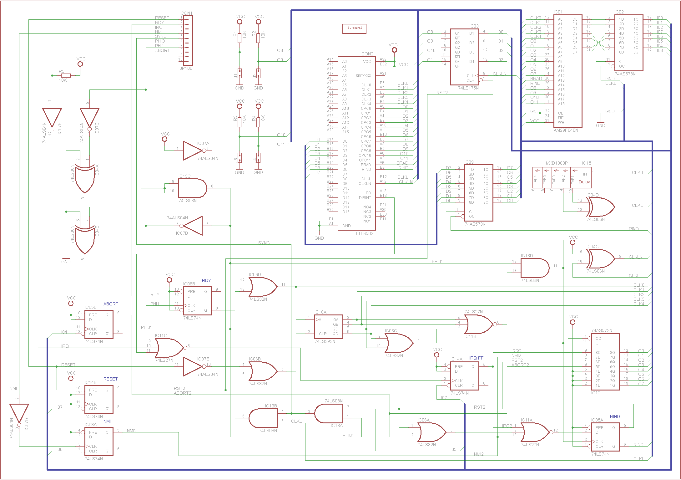
Card #1

CPU in/output
This board is the actual interface to the outside world. Connector CON3 represents the 6502 and CON4 the 6510. Why a 40 pins header? I already have a cable laying around with a 40 pins header on one end and an IC like connector on the other end.Using a header has another advantage: it is easier to connect the card directly to other boards, in my case my own test card, card #10.
PHI0 comes from the host system and goes to card #2 through connector CON3. Card #2 generates PHI1. For several reasons I decided to generate the outgoing PHI2 on this board using inverter IC07b. Why not using PHI0 as source for PHI2? At this moment I use my experience gathered with my project 6502 -> 65816. A real prototype can confirm whether I am wrong or not.
The basic idea is simple:
- Two 573s, IC02 and IC03, take care of latching and buffering the address bus. Why latching? Sometimes the bus is needed temporarily for other things and in this way the address is maintained.
- A 573, IC04, takes care of reading and latching the data coming from outside. Why latching? To make sure the data is also available to the TTL6502 after PHI0 has become (L).
- A 573, IC05, takes care of latching the data and presenting it to the outside world.
Tristating the buses
The 6510 and an Atari version of the 6502 can be tristated. 573s have an OC input that takes care of that. The 6510 and the Atari version go into tristate mode the moment AEC/BE becomes (L). A 573 is active the moment OC is (L). This means an inverter is needed: IC07d.The R/W has to be tristated as well: IC11c, a 125 buffer, takes care of this.
ID signal I123 takes care of enabling IC05, the 573 that outputs the data. IC06c, an OR gate, makes sure that IC05 is tristated as well during a tristate demand from the outside world.
Supporting the 6510
The major difference with the 6502 is the 6-bits onboard I/O port. An added 6526 takes care of that. The 6526 may only be visible at the addresses $0000 and $0001. Two 688s, IC08 and IC09 take care of that. Signal I121 and OR gate IC06a take care of the fact whether the 6526 will be enabled at all or not.When reading from $0000 or $0001, we must make sure that there is no conflict with IC04, the 573 that reads the data from the outside world. Inverter IC07c and OR gate IC06b take care of that.
Card #2
Input from card #1
This board contains the circuits needed to generate the input signals for the Instruction Decoder FlashRAMs. Therefore it needs some outside inputs like Reset and interrupts. Connector CON1 takes care of that and connects directly to connector CON1 of card #1.One of the most important inputs of the TTL6502 is PHI0. Because it must serve as input for many other gates in my design and not being sure if this will stress the original system, I decided to buffer it first with IC13d, a left over AND gate.
PHI1 is created by inverting PHI0 (IC07b). The PHI2 needed for this card is generated by inverter IC07c. Two EXOR gates delay the result (see later).
The Instruction Decoder
The main parts of the ID are the FlashRAMs that I mentioned several times. The second part is a number of 573 or 574 latches. These latches are used to prevent glitches because glitches can be fatal. For example, the ID must reset the opcode step counter at the end of an opcode. Imagine a glitch that resets the counter prematurely; the processor will start to execute a new opcode but not having completed the previous one, this could be the start of a disaster.Dealing with the access time and glitches of the FlashRAM
The latches have to be triggered by a pulse the moment we are sure that the signals outputted by the FlashRAMs are stable. First we have to deal with the access time itself. My idea: use a delay line IC (IC15) from a scrapped PC. This IC outputs the input signal at different timing intervals at several output pins.
IC15 is fed by CLK0. The needed pulse is created by feeding the outputs of two taps of the delay IC to an EXOR gate. This gate outputs the difference in time between these outputs as a pulse:
               ____________________                      ________________
PHI0      ____|                    |____________________|
              .    .
              .    .____________________                      ___________
TAP1      ____.____|                    |____________________|
              .<-->. = access time
                       ____________________                      ________
TAP2      ____________|                    |____________________|

                    __                   __                   __
EXOR      _________|  |_________________|  |_________________|  |________
The 574's can do with the rising edge of this pulse. EXOR gate IC04c inverts the result and this pulse is fed to the backplane. Some other cards have good use of it.
The counter circuit
The opcode itself is a collection of several micro instructions. Some of these micro instructions can be executed parallel, some have to be executed in a certain order, read: at the right step. The counter tells the ID what step has to be executed.The base part is IC10a (393: 4 bits binary counter with clear). Together with PHI2 we now have a five bits counter where PHI2 is the LSB, now called CLK0. These five bits, good for 15 clock cycles/31 steps, are directly fed to the backplane and serve as inputs for the FlashRAMs of the ID.
The outputs of the 393 are also fed to a 4 input NOR gate, a gate created out of an OR gate (IC06c) and a 3 input NOR gate (IC11b). At the end of an instruction the 393 is cleared and all its output become (L). At that moment the output of this 4 input NOR gate becomes (H). This output is ANDed with PHI0' using AND gate IC13c. The output of IC13c is used as trigger to latch the data into two 573s, IC09 and IC12 (see later).
Resetting the counter
The idea is that two things have to be done at the last cycle of an instruction:
- prepare the TTL6502 to read the opcode of the next instruction
- reset the counter
The last is done by setting ID output I05 (H). After some processing I05 is used to clear the 393. What kind of processing has to be done?
First, the Reset signal must be able to reset the counter as well. So before the signal reaches the 393, it has to be ORed (IC06b) with the inverted (IC07e) Reset signal. The effect is that an active Reset simply keeps the 393 in reset mode, it will output 0000, as long as the reset signal is active.
Second, once the counter has been resetted by I05, the clear signal must be disabled again before the falling edge of PHI2 otherwise the 393 won't be able to count at all. We just happen to have such a signal in our system that can do the trick: the pulse for the FlashRAM latches. The AND gate IC13b reduces the actual clear signal to the size of the pulse for the FlashRAMs.
Setting I05 can be done any time. If done on count xxxx0 it won't do anything because it is mixed with PHI0 first, see later. If done on count xxxx1, the counter turns into count 00001. But, as the FlashRAMs already have been latched, nothing will happen any more. And that is the reason the last cycle of the previous instruction has to prepare the decoder to read the opcode of the next instruction.
Now I05 has to be cleared again. This is done at the latch of count 00010. But that won't happen immediately at the moment the FlashRAM pulse becomes (H) and so we run the risk that the 393 is reset again by another, now unwanted pulse. By ANDing (IC13a) I05 with PHI0' we make sure it is already disabled at forehand.
Latching the Opcode, Reset, NMI, IRQ and Abort:
IC09, a 573 8 bits latch, is the so called Instruction Register: it latches the opcode. The opcode is only present at the first cycle. The Instruction Register makes sure that the opcode is present at the ID for the other cycles as well. Another 573 (IC12) does the same for Reset, NMI, IRQ and Abort.NMI
NMI, a negative edge triggered interrupt, is inverted first (IC07f) and fed to the CLK input of a 74 D-flipflop (IC08a). Why not tying NMI directly to PRE and saving a gate? At the end of the process the ID has to reset the flipflop. Using PRE as input would immediately set the flipflop again and thus forcing the decoder to repeat the whole process.
After handling NMI, the flipflop is resetted by I06.
Abort
One idea was to emulate the 65816 as well. But I'm not familiar enough with this CPU so I decided to skip this idea. But I had already designed this circuit using gates that just happened to be left over. So with discarding it now I wouldn't gain anything.
For the rest I can be very short: Abort is treated in the same way NMI is. IC07c is the inverter, IC05b the flipflop and I04 the reset signal.
IRQ
IRQ is a level triggered interrupt and it is only checked at the end of PHI0. IRQ can also be disabled. NOR gate (IC11a) serves all these demands in one go. If the IRQ is still active (L) at the end of PHI0 and the disable bit is inactive (read: low) as well, then the moment PHI0 becomes (L) the rising edge of the output of the NOR gate will trigger the D-flipflop.
After handling IRQ, the flipflop is resetted by I07.
Reset
Reset doesn't suffer the above problems because the counter cannot start until the Reset signal is inactive again. Therefore it can be connected directly to the PRE input.
After handling Reset, the flipflop is resetted by I07. Yes, this is the same signal as for resetting the IRQ flipflop. The idea behind it: resetting the Reset flipflop at any other point in time won't have any effect so why not using an existing signal? For the same money I could also have used I06, the NMI one.
If for one or another reason the system is resetted the moment I07 is (L), there is a possibility that the flipflop will toggle its outputs and thus presenting wrong information to the latch and other parts. But that is no problem because during a normal run count 00000 can normally only occur during a reset. In that case the ID has been programmed to reset all outputs to default values: I07 will be set (H).
The further processing of Reset, IRQ and NMI
The four \Q outputs of the flipflops are latched by a 573 (IC12) at step 00001 and NORed by IC06a and IC11c. If one or more of these signal are (H), IC11c's output becomes (L). The output of AND gate IC13c, that is used to latch the data into IC12, is also used to clock D-flipflop IC05a. The flipflop latches the output of the NOR gate.
The outputs of this flipflop now either activate the outputs of IC09 (= opcode) or those of IC12. One of these signals is RIND, the signal that tells the ID whether an IRQ, NMI or Reset is going on or not.
Why is D-flipflop IC05a needed? Just like the opcode or the above signals the output of IC11a can change in the middle of an instruction and therefore has to be preserved as well. We cannot use a free pin of IC12 because it isn't available all the time, so we have to use a separate latch; IC05a in this case.
SYNC
SYNC tells the outside world the first cycle of an opcode is being processed. Just by coincidence the output of IC13a is exactly what we need.ReaDY signal
RDY is a signal to tell the 6502 to halt as long as RDY is (L). The outputs of the 393 are increased at every falling edge of PHI2. The basic idea is that RDY prevents PHI2 to reach the counter. Before PHI2 is fed to the 393, it goes through an OR gate, IC06d. This gate ORs PHI2 with the \Q output of IC08b, a 74 D-flipflop. This D-flipflop represents the state of RDY at the end of PHI0 and does this by saving the state of RDY at the rising edge of PHI1. If RDY is (L), output \Q becomes (H) and will block all pulses from PHI2 towards the 393 and ID by keeping CLK0 (H).I mentioned before that I use two obsolete 86 EXOR gates to delay PHI2. Why? There are several delays in the circuit and I just want to be sure that the output of \Q reaches the OR gate IC06b before PHI2 does. If it wouldn't do so, there is a change that the OR gate still could output a (L) pulse long enough to make the 393 count.
Extra opcodes
As said before I only need 15 inputs for my Instruction Decoder. Using 29F040s or equivalents means I have 4 left over inputs that I can use for extra opcode set and/or processors. A 174, 4-bits D-flipflop, takes car of this.The extra ID bits are set at step 00010. At the rising edge of the negative ID latch signal the data is copied from the D inputs to the according Q outputs. And on their turn these outputs control the extra ID inputs. The next stage is acting if this was just a one-byte opcode, thus preparing the ID for reading the next opcode from the data bus and resetting the counter.
The read byte will be treated as just another opcode. Assuming that at least one of these just set ID bits isn't (L) anymore, the according instructions for this opcode are read from another location inside the FlashRAM and therefore can be completely different from those of the original 6502.
Although the schematics say to use 29F040 FlashRAMs for the ID, I don't have enough of them and will use 29F020s. This is still enough for seven extra instruction sets. But how to use them? The 6502 has some so called KILL opcodes; when executed, these opcodes will freeze the 6502 completely. We can use these opcodes to create two-byte opcodes.
If compatibility is a must, then we can use one of those KILL opcodes and a combination of two and three-byte opcodes. But which one? The 65816 hasn't any illegal opcodes anymore but there exists an unused opcode: WDM. WDM stands for "William D. Mensch", the designer of the 6502 and 65816. This code was meant to be used in future 65xxx CPUs. My idea is to use this opcode as base for the multi-byte instructions.
When emulating other processors using the same set of FlashRAMs, I already need to point the ID to another location inside the FlashRAM at Reset. This can only be done by setting (a part) of the extra opcode bits O8..O11 by hand. This is done by lifting the according output pins of the 175 out of their sockets. Resistors R1..R4 pull the lines (H). Jumpers J1..J4 enable you to set the right combination to select the wanted processor.
Remark: for the moment this only works with 6502 equivalents like the 65C02 and 65SC02. To emulate a Z80 for example, you will need its equivalent of Card #1.
Eurocard #3
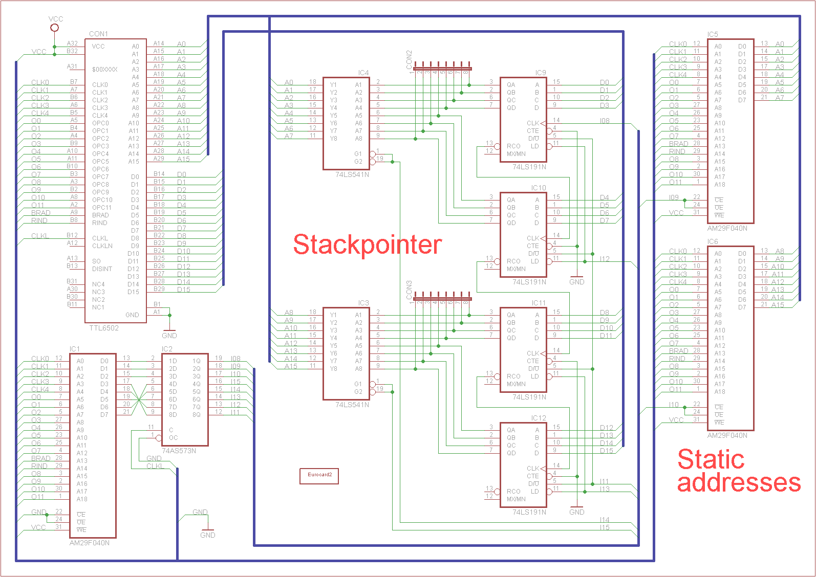
This card contains:
- the Static Address generator
- the Stack Pointer
The Static Addresses Generator (SAG)
After a reset, the address $FFFC has to be generated in some way. Something equal has to happen with a NMI or IRQ, or when the Zero Page or Stack is accessed. IC5 and IC6, two FlashRAMs, provide the needed address bits.These FlashRAMs are fed with the same signals as the FlashRAMs of the ID. For the few addresses they have to provide, this looks like overkill. But an earlier design used at least five 541's and 244's which inputs were wired according the needed addresses. This solution is simpler, needs less ICs, occupies less space and is also more flexible for future use; think of the 65816, Z80, 6800 and 6809 with extra and different addresses.
Although both ICs know what bytes needs to be outputted, they cannot control their own output. That is something the decoder still has to do (I09 and I10).
The Stack Pointer
The Stack Pointer (SP) takes care of providing the address when pushing data to the stack. The heart of the SP is made out of two pairs of cascaded 191s (IC9..12), preloadable 4-bits binary up/down counters. Because the counters don't have any tristate capabilities, two 541's 8-bit buffers (IC4, IC5) have been added to provide this function. I also added some connectors between the 191's and 541 that enable me to read the output of the 191's using 7-segments LED displays.Why two pairs of 191s, this make 16 bits? Indeed the 6502 has only an 8 bits SP but the 65816, Z80 and 6809 have a 16 bits one.
Remark: the HB part can be set to $01 at a reset. But when emulating a real 6502, any program is able to clock the 16 bits SP beyond $FF or under $00. In that case the HB part will change as well, something that cannot happen in a real 6502. Therefore in 6502 mode the HB part has to be disabled and in its place the HB of the SAG will generate $01.
Eurocard #4

This card contains:
- the Program Counter
The Program Counter
The Program Counter (PC) takes care of the address lines during normal operations. As you can see, the design looks like the one of the SP. The heart of the PC is made out of four cascaded 191s (IC7..10). Originally it was planned that TTL6502 would only use them in the "count up" mode. Having the ABORT signal of the 65816 in mind and at the cost of only one ID output, I also provided the means to count backwards.Again, because the counters don't have any tristate capabilities, two 541's 8-bit buffers (IC3, IC5) have been added to provide this function. I also added some connectors between the 191's and 541 that enable me to read the output of the 191's using 7-segments LED displays.
The two 573's (IC11, IC12) are needed when the PC has to be fed with a new address. For example, in case of the JMP instruction the new address has to be stored temporarily because, during loading the two bytes, the original address is still needed. The ID takes care of copying their contents to the 191s at the end of the instruction.
If an interrupt has to be served, the SP must take over the address bus to be able to save the original address. So the SP must be able to read this address somehow. Two 541s, IC6 and IC6, take care of that, they output the momentary address of the PC to the data bus when needed.
Eurocard #5

This card contains:
- the registers A, X and Y
- the address lines A16..23
The Registers A, X and Y
With the future in my mind, I decided to create 16 bits registers. Each 16 bits register is made out of two 573s and two 541s. Why not only using 573s? Like with the SP and PC, the combination enables me to read the contents of the registers on the fly using 7-segments displays, something impossible when only using 573's.The address lines A16..23
I mentioned before I had the idea to emulate the 65816. It has two registers for handling the address lines A16..23:- the Program Bank Register (PBR)
- the Data Bank Register (DBR)
The 6502 can only handle 64 KB of memory. The registers enable the 65816 to handle 256 nonoverlapping segments of 64 KB each. The PBR points to the 64 KB segment where the program is running. One way to change that register is executing a long jump:
JML $123456
The rest of the program will run inside this segment.
The DBR points to the 64 KB segment where the data has to be read from or written to and is only used for that specific command:
LDA $123456
Original 6502 commands like
LDA $789A
will only handle data within the segment where the program is running.
As said before, I had the intention to emulate the 65816 as well but changed my mind. The reasons are quite simple:
- I have only one computer equipped with a 65816, an Apple II GS. But I have lot of 6502 computers and Commodore 64s.
- I simply don't have enough knowledge of the 65816 yet. And the more I learn about it, the more I doubt that I can emulate it with this design.
But the address expansion is usable: I have always dreamed of a CBM 8032 with 512 KB of memory running my own 6502 Pascal.
Eurocard #6

This card contains:
- an 8 bits ALU
- a 16 bits ALU
The ALU
The ALU, short for Arithmetic Logic Unit, wouldn't have been a problem if the 6502 hadn't this decimal mode. But it has and so far I haven't heard of any ALU-IC capable of dealing with this mode. So soon the idea rose to use EPROMs and later FlashRAMs.The ALU needs to be able to handle at least the next commands:
- ADC
- ADD
- AND / BIT
- ASL
- CMP / CPX / CPY / SUB
- DEC / DEX / DEY
- EOR
- INC / INX / INY
- LSR
- ORA
- ROL
- ROR
- SBC
Four selection bits will cover the above 14 commands. An extra bit is needed to deal with the decimal mode. It has to be an extra bit because it is an external input coming from the Flag Register.
Needed inputs
- Zero flag- Carry flag
- Decimal mode flag
- 4 bits 1st operand
- 4 bits 2nd operand - 4 command bits
As you can see I only use 4 four data bits as input. Using 8 bits would mean I would need a FlashRAM with at least 23 inputs. It is possible that it exists but I don't have or know one (that is, not in +5V). By cascading two FlashRAMs I get the same result.
Only needing 15 inputs now would mean that a 29F010s is more than perfect for the job. The two extra input bits make sure I don't have to worry about implementing extra commands.
But this trick however has one disadvantage: cascading two FlashRAMs with an access time of 70 ns would mean a total access time of 140 ns, meaning that I can forget about a 4 MHz system and maybe about a 3 MHz one..
When working things out I again got into a bit of trouble. In my first design I used the Carry output to tell the next FlashRAM about the result. But then I noticed that in case of a shift to the right, like ROR and LSR, its predecessor should know about it. To make it worse, in case of ROR the Carry bit is copied into the last bit and the first bit is copied into Carry. The difficulty is that the place where we find this last bit depends whether we work in 8 or 16 bits mode. Have a look at the next table:
task            IC5          IC6          IC7          IC8
-------------------------------------------------------------
Add, etc.    ext. Carry      IC5          IC6          IC7
ROR 16 bits     IC6          IC7          IC8       ext. Carry
ROR  8 bits     IC6       ext. Carry       -            -
Two 257s, quadruple 2-to-1 multiplexers, take care of this. ID output I46 selects between the 'previous' or 'next' Carry, I47 selects the 8 or 16 bits version.
Each FlashRAM outputs 4 data bits, a Carry bit, an Overflow bit and a Zero bit. One bit is unused. The overflow bits of the first and third FlashRAM are not used of course.
Both operands are stored in a 573, IC12 and IC13. Because these ICs don't have to share their output with other ICs, only a clock signal is needed; I40 and I41.
A 245 buffers the result towards the data bus. Although the FlashRAMs can be tristated as well, the idea is that the resulting flags still have to be available after that the FlashRAMs were read. Signal I44 enables the 245 to output its data to the internal data bus.
A 16 bits ALU
You probably already noticed some hints about the 16 bits version of the ALU. Wanting to create a 16 bits 6502 also means I need a 16 bits ALU. I will need it at least to check whether a 16 bits number is zero or not. In the beginning I thought that cascading another two FlashRAMs would ruin my "at least 2 MHz" goal. But after some time I suddenly realized that, in case of a 16 bits calculation, I was completely free to insert one or two wait states. OK, I would loose one or two cycles but the whole execution would always be much, much faster then two complete 8 bits calculations. Problem solved :)The HB part of the ALU is a just a copy of the LB part, so nothing exciting there. But because this expanded 6502 can operate in 8 bits as well as in 16 bits mode, we need to be able to feed the Flag Register with the correct flag information at the right time. IC11, a 257 2-to-1 multiplexer, takes care of that.
Eurocard #7
This card contains:
- the Address Adder 8 bits operations
- the Address Adder 16 bits operations
- indirect addressing
The Address Adder 8 bits operations
When executing a branch, the final address has to be calculated by adding the just read byte to momentary address. If this is a forward branch, it could be done by the original 8 bits ALU. But if it is a negative one that doesn't cross a page border, we need a fast 16 bits adder. I have found solutions that could have worked for the original 6502 but certainly wouldn't work for the 16 bits version.So we are looking for a 16 bits adder and I already can hear you say: "No problem, we already have one!". But using the ALU mentioned above with its huge access time, I can surely forget about 2 MHz operations after all because the whole calculation has to be done within one single step :( Another problem, it also would mean I would have to add more hardware to the ALU card and I simply don't have the place for it.
So how can I calculate that fast without using the ALU? My only idea was designing a separate adder. The basic idea is quit simple: four cascaded 83's (4 bits full adders), IC10..13, do the trick. But because they don't have tristate outputs, two 541's (IC5 and IC6) were added to complete the design.
IC7 and IC8, two 573s, latch the address on the address bus in case of a branch and can output their data to the 1st operand of the 83 adders. IC18, another 573, latches the LB data meant for 2nd operand of the 83 adders. In case of a branch, a byte has to be read from the first. But this is a special byte, a so called 'signed' byte; bit 7 tells whether the byte has to be added to or subtracted from the address. In the first case the HB has to be zero, in the last case the HB has to be $FF. This is realized by IC20, a 541 buffer, an AND gate, IC26a. The output of the AND gate is used as input for all of IC20's inputs. One of the AND gate's inputs is bit 7, the other I63, an ID output. If I63 is (H), bit 7 decides whether IC20 outputs $00 or $FF. If I63 is (L), IC20 always outputs $00. The last is needed indexed operations like 'LDA $1234,X'.
When a branch has to be taken, the result has to be fed into the Program Counter again. IC22 and IC23 take care of that by feeding the result to the data bus where the PC on its turn can copy it.
When a branch has to be taken and a page boundary is crossed, the original 6502 needs an extra cycle to calculate the new HB of the address. The Carry output of the second 83, IC11, will become (H) if this is the case. This signal is fed to the backplane where the Flag Register card will pick it up.
The Address Adder 16 bits operations
Because the TTL6502 supports 16 bits registers, it's logical to assume it will support 16 bits indexed operations. IC21, a 573, takes care of this.Indirect addressing
Have a look at the instruction 'LDA ($12,X)'. We first have to add the content of register X to $12 and to output the result to the address bus. This means we need to store this $12 somewhere first: IC17, a 573. The result will be outputted by the LB output of the adder, IC22. The HB of the SAG will output the $00 needed for the zero page.The byte to be read is the LB of the address where the actual data can be found. But where should we store it? Let's assume a simple solution: a 573 with its inputs connected to the data bus and its outputs to the address bus.
Next the HB has to be read. But for this the address that is outputted by the adder has to be increased. The way to do it is quite simple: each 83 adder has a Carry input and the one of the first 83 was set to (L). By setting it (H), the outputted address is increased automatically by one.
The byte to be read now is the HB of the address where the actual data can be found. Again we can store it in a 573.
Disabling the adder and enabling the two 573 mentioned above, enable us to read the wanted byte. So far no problem. But in case of the instruction 'JMP ($3456)' I need to be able to read two bytes at the end. And that is impossible with this 'just two 573s' solution.
My solution was adding these 573s between IC15 an IC17 and the data bus. So in the above explanation $12 is first read by IC16 but immediately outputted to IC17. So at the end IC16 and IC14 contain the LB and HB of the final address. When needed they output their data and now IC15 and IC17 latch the data and immediately output it to the adder.
It seems quite logical that the adder must output these bytes but then, what about the 2nd operand? There isn't one, or better, we must make it $0000. IC20 takes care of the HB and IC19, another 245 but with its inputs tied to GND, takes care of the LB.
So far IC15, a 573, hasn't been explained. Please, have another look at the instruction 'JMP ($3456)'. In this case $56 has to be stored in IC17, just like $12 above, and $34 has to be stored in IC15, the HB part. As there is nothing to add here, we will use $0000 circuitry, IC19 and IC20, in the first stage as well.
Remark #1: AFAIK in the 6502 the above construction is only needed for the indirect jump. But when I started to think about reading or writing 16 bits, I found out that the Carry trick was needed here as well.
Remark #2: Analyzing "ORA ($12,X)" I found out that the 6502 first reads a byte from ($12) while in the mean time adds X to $12. It looks that the 6502 indeed uses the ALU. OTOH this means that the TTL6502 can be faster. But to remain compatible I maybe have to add one or more dummy cycles.
Eurocard #8
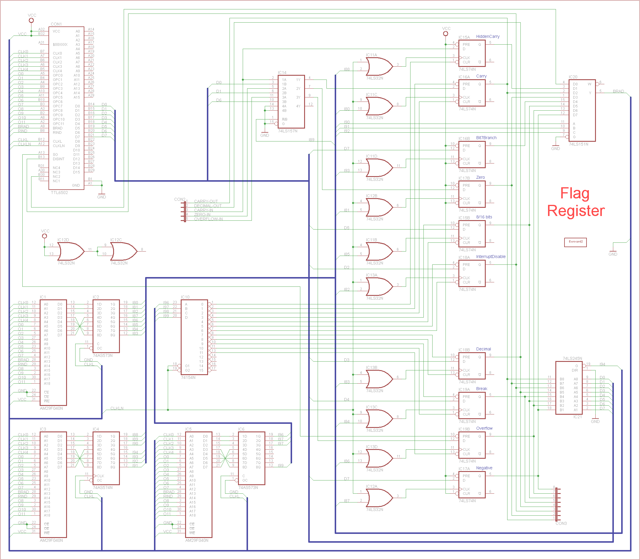
This card contains:
- the Flag Registers
The Flag register
Most possibly the first impression will be: this is a huge design! Yes, it is, and with reason. This design enables the TTL6502 to update one or more registers in just one step. The 6502 and the M02 mentioned above need more.The core of the Flag register (FR) is made out of ten 74 D-flipflops (IC15..19). Seven of them are part of the official FR, the other three are needed for other functions.
In some cases the Data input is only fed by data from the internal data bus, in other cases it can be either the data bus or data coming from the arithmetical bits Zero, Carry or Overflow from the ALU (card #6) and in one case it is just fed with the Carry from the ALU. IC61, a 157 2-to-1 multiplexer, takes care of choosing between the data and the arithmetical bits.
As said, every flipflop has its own clock signal. In this way it is possible to change just one single bit or even the complete register in case of a memory move (PLP, RTS, RTI). The 'Overflow' flipflop is the only one that can be set by an external signal, SO in this case.
When using an opcode like CLC only one bit has to be set or reset. So far I don't know of any opcode where you have to set or reset more than one bit in one step. This means that one 154, 4-to-16 demultiplexer, can serve our purpose to set or reset any bit where needed.
Not being sure if such a (re-)set signal can interfere with an operation at the next step, I decided to feed the enable inputs of the 154 with the negative ID latch signal. It is long enough to perform the wanted operation and the situation is stable long before the next step.
Sometimes one or more bits for these flipflops originate from an external source; think of the Carry, Negative and Zero bit of the ALU or opcodes like PLP. What must be done to clock them into the flipflop? The clock input of every flipflop has been connected to its own OR gate. One of the OR gate's input has been connected to an output of the ID, the other to CLKLN, the negative ID latch signal. If the ID bit at the first input of the OR gate is (L), the rising edge of the negative latch signal will clock the bit found at the data input into the according output.
And now the reason why the design is so big: because I thought that all operations had to be done within one step. But have a look at this: all 6502 one byte instructions take two complete cycles. And I always wondered why. A possible explanation is that I did a too good job and that the real 6502 needs two or more steps to handle the FR. This is something the M02 does, it indeed needs (at least) two steps to update the FR. But at the other hand it needs less hardware.
In case of a branch the ID needs the state of a particular bit to decide whether the branch should be taken or not. A 151 8-to-1 multiplexer, IC20, enables the decoder to select the flag needed for a particular branch. The result, BRAD, is fed to the ID.
BRAD is not only used for deciding whether a branch should be taken or not, but also for deciding whether a branch instruction takes two or three cycles.
A 245 buffer, IC21, enables the TTL6502 to read the contents of the Flag Register.
In a real 6502 bit 5 isn't used, in a 65816 it is. I just happened to have a left over flipflop, so why not use it? The original idea was that a free input at the 151 multiplexer enabled this bit to use BRAD to tell the ID if an 8 bits or 16 bits operation had to be performed. But to be honest, I have my doubts if this would work out right.
Anyway, I never liked the way the 65816 switched between the 8- and 16 bits mode. I personally prefer the use of separate mnemonics for the 16 bits mode. But if I ever change my mind, the circuit is present.
Addition: a) I completely forgot about the Emulation bit and b) it seems that there isn't just one bit that controls the 8/16 bits mode but two. So: "Goodbye, 65816, hello my own 16 bits 6502" :)
Eurocard #9

This card contains:
- 16 bits expansion
More "Expanding the 6502"
As already said many times, using the faster and bigger FlashRAMs gave me the possibility to expand the 6502 with extra opcodes and other nice features. The 16 bits registers are one of them. But the TTL6502 still has only an 8 bits data bus to the outside world. So a way had to be found to read/write the upper bytes from/to the original data bus. Two 573s, IC9 and IC10, take care of this.Even more registers
Another CPU that I have in mind to emulate is the Z80. But the fact is that the Z80 has a lot more registers than the 6502 has. I could solve it by adding more and more 573/541 pairs (or just only 573's) but that would cost a lot of board space. So the idea rose to use two 2 KB SRAMs. One FlashRAM is able to handle 32 16 bits registers.
But thinking things over I realized I had a problem: how could I perform a register-to-register transfer within these SRAMs? There is no way a SRAM can output a byte and store it at another address at the same time. This meant I needed a Temporary Data Register (TDR) to perform the whole transfer in two steps: two 573s, IC5 and IC6.
At this moment I only access 16 registers. Connecting more address lines of the RAMs to the ID would mean I could access up to 2048 registers. One solution is adding another FlashRAM/573 combination. A second one is using left over ID outputs from other cards.
Having all those extra registers, how am I going to use them? I have some, but only vague ideas. Input from you is welcome!
Eurocard #10
I use an I/O ISA card to test everything. It is quite possible that you don't have this card but the next part can give you ideas to create your own test device.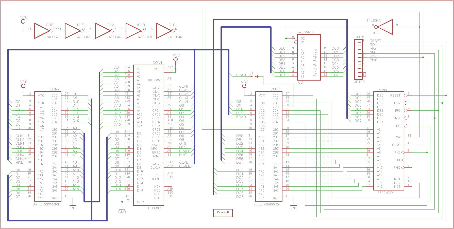
This card contains:
- the test card
Testing everything
One question to myself was: "How do I test everything?". Not just the whole design but also every single card. I just happened to have some PC ISA cards with four 8255s on them. These four 8255s are good for 96 input and outputs, presented to the outside world by two 50-pins headers, CON1 and CON2.In my design the two 8255s behind CON1 are used to simulate the host system. This done by connecting it to the 6502 connector on card #1 through connector CON 3.
As you can see I use two ports for the data bus: one to write data, the other to read data. A 541 buffer, IC2, buffers the data towards the TTL6502. The idea is quite simple: when the TTL6502 performs a write operation, the R/W line will be (L) which on its turn, with the help of inverter IC1d, will disable the 541. During a read operation the output of IC2 will be enabled and the TTL6502 can read the data.
People who are familiar with the 8255 may wonder why I did it this way; a port can also be programmed to be either input or output. In most cases the TTL6502 is in read mode and therefore the PC will be in write mode. The problem is that the PC only then will notice that the TTL6502 has gone into write mode when the R/W line becomes (L). The detection has to be done by polling and that will take time. And once the PC has found out about the new situation, it has to reprogram the control port of the 8255. And this will also take time. And all that time long two ICs are outputting data on the same bus.....
The two 8255s behind CON2 and one port of CON1 are used to either monitor the signals on the backplane or to generate them if the responsible card isn't present. Whether a port is in read or write mode depends partly on what card is tested and partly on what action is needed. If the Instruction Decoder is not amongst the cards to be tested, CON2 will generate them, otherwise it only has to read the signals.
A small problem is BRAD, the signal that helps the ID to decide whether a branch has to be taken or not. If the FR isn't present, the computer must generate it, in this case using output pin Con1 2C3. If the FR is present, it only has to be read. The problem is that, in contrary to the 6522 or 6526, you cannot select a single bit of a port to be input or output. This can only be done in blocks of four or eight bits.
So if the FR is present, we use Con1 port 1C as an input. Jumper J1 then takes care of making sure that both signals won't clash.
The backplane
The backplane is the connection between all boards. As base I'm using 64-pins AB-DIN connectors. The pin out:- 2 * +5 Volt
- 2 * GND
- 16 * internal address bus: A0..A15
- 16 * internal data bus: D0..D15
- 5 * counter for the ID
- 8 * opcode for the ID
- 1 * branch signal for the ID
- 1 * Reset/IRQ/NMI signal for the ID
- 1 * latch signal for the ID
- 1 * inverted latch signal for the ID
- 4 * future expansion for the ID
- 1 * external SO signal for the flag register board
- 1 * disable interrupt signal from the flag register board
- 1 * first 64 KB selected - 4 pins for future use
Emulating the 65816
During some time I had the idea of supporting the 65816 as well but I later dropped it. One of the reasons of discarding the 65816 was that I also needed inputs for telling the ID that either an 8 or 16 bits operation was going on or that the Emulation bit was set or not. And in the pre-FlashRAM period I simply disliked to loose too may inputs to a processor that I didn't know well enough yet. The extra outputs of the 65816 were another problem.Using FlashRAMs, and thus having these extra inputs now, could revive the idea again. But to be honest, I prefer to create my own 16-bits 6502.
A much simpler design
So far I used a lot of registers for various purposes. I'm not only talking about A, X and Y but also about those registers used by the Adder, SP, PC and even the Flag Register itself: they all could be brought back to a single 2 KB SRAM. For example: The core of the PC and SP is the 191 which is nothing more than a register with an extra feature: it can count up or count down. We have something that can do exactly the same: the ALU. We have to increase the PC? We first read the stored value from the SRAM, increase it using the ALU, store the result in the SRAM and also store it in the address buffer. Job done! The same story can be used for the SP. As you can see the ALU will still be needed but it will be an 8-bits version.But I guess that you already understand there is the price that has to be paid for simplifying the design: less speed.
You are curious? Please have a visit:
the Mini6502
You can email me here.